|


|
|
|
||||||||
Tenting Via In Pad - Yes or No?
Board Talk
|
||||||||
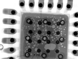
TranscriptPhil And welcome to Board Talk with Jim Hall and Phil Zarrow of ITM Consulting, the Assembly Brothers. We are coming to you from high atop Mount Rialto at ITM headquarters. We are here to talk about electronic assembly, materials, equipment, components, practices, procedures, and who knows what else. So Jim, what else? What are we talking about today? Jim Okay, this comes from N.P. Should the thermal vias on the bottom terminated components be tented on both sides to prevent flux trapping and solder wicking or is it sufficient to tent on the top side only, or should the vias just be plugged? Phil Good question. Jim This is a well talked about topic. Under all circumstances you have to prevent solder wicking. We are talking about the large sensor ground plane or thermal plane in the center of a bottom terminated component. We are talking about the pad for it on the printed circuit board. Because most of these are used as thermal pads that dissipate the heat, to get the heat away from the top surface we put vias into the pad to conduct the heat down into the PCB. Thus keeping the IC in the BTC package cooler and operating correctly. Okay, so now we are going to go solder this. We are going to put a lot of solder paste on there. We have these holes, plated through holes right in this large ground plane. What do we do? We cannot allow solder to wick into those holes because bad things will happen. One of the worst things is that whatever is going to happen is not going to be consistent. Sometimes maybe no solder will wick into a hole. Other times a lot of solder. Sometimes it will create a big void. Sometimes it won't create any void. If we look at published data with cross sections and x-rays you will see the same part with an array of vias, some of them are wicked and some of them aren't. So you need to prevent that. Now, how to deal with via in pad. The IPC specs talk about six or seven different ways. Some of them are capping, top capping on the bottom, or tenting I think is the term, or filling. The belt and suspenders way is to fill the entire through hole and actually plate over it with copper on the top. So if you look at the top surface of the pad, you don't even know the vias are there. Then you have no issues, you are just soldering to a flat copper surface. Some houses actually fill the whole barrel. But that is the most expensive. There are a limited number of houses that will do that. Some houses actually fill the whole barrel with copper to improve the thermal thing. Then there are tenting and so forth, or solder masks or other materials filling. Different people have had success with just about all of them, but with tenting there have been problems where they don't maintain the seal and stuff still get in there and bad things still happens. You need to be concerned. You have to prevent that solder wicking. How you do it is a process you have to work out with PCB suppliers and your cost considerations. One thing that is being looked at a lot now is to not tent the via but to just put an annular ring of solder mask around it and when you design the stencil not print paste on the hole so you don't get any wicking there. You don't worry about actually filling the via. You just prevent through solder mask a ring around the hole to prevent the solder from wicking down there. There is a lot of published literature. I could spend hours talking about all of the different things that have been investigated. Whatever you do you have to come up with a system. Printed circuit board suppliers can provide you process to work with to prevent the voiding which can hurt your thermal transfer and if your using it as a ground plane for an RF circuit. Phil Very well put, my brother. And I think you sufficiently answered that question. You have been listening to Board Talk with Jim Hall and Phil Zarrow. We appreciate your listening and hope you learned from it. One thing you should definitely learn is whatever you are doing with your vias, tented or otherwise don't solder like my brother. Jim Don't solder like my brother. |
||||||||
Comments
|
||||||||


|

|

|